MRF6VP121KHR6 MRF6VP121KHSR6
7
RF Device Data
Freescale Semiconductor
TYPICAL CHARACTERISTICS
23
1
0
100
17
70
60
50
40
30
Pout, OUTPUT POWER (WATTS) PULSED
Figure 10. Pulsed Power Gain and Drain Efficiency
versus Output Power
G
ps
, POWER GAIN (dB)
η
D,
DRAIN EFFICIENCY (%)
ηD
16
1000 10000
25_C
TC
=--30_C
85_C
20
18
Gps
19
20
21
10
10
VDD
=50Vdc
IDQ
= 150 mA
f = 1030 MHz
Pulse Width = 128
μsec
Duty Cycle = 10%
22
250
109
90
TJ, JUNCTION TEMPERATURE (°C)
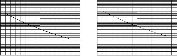
Figure 11. MTTF versus Junction Temperature --
128
μsec, 10% Duty Cycle
This above graph displays calculated MTTF in hours when the device
is operated at VDD
=50Vdc,Pout
= 1000 W Peak, Pulse Width = 128
μsec,
Duty Cycle = 10%, and
ηD
= 56%.
MTTF calculator available at http://www.freescale.com/rf. Select
Software & Tools/Development Tools/Calculators to access MTTF
calculators by product.
107
106
104
110 130 150 170 190
MTTF (HOURS)
210 230
105
108
250
109
90
TJ, JUNCTION TEMPERATURE (°C)
Figure 12. MTTF versus Junction Temperature --
Mode--S
This above graph displays calculated MTTF in hours when the device
is operated at VDD
=50Vdc,Pout
= 1000 W Peak, Mode--S Pulse Train,
Pulse Width = 32
μsec, Duty Cycle = 6.4%, and
ηD
= 59%.
MTTF calculator available at http://www.freescale.com/rf. Select
Software & Tools/Development Tools/Calculators to access MTTF
calculators by product.
107
106
104
110 130 150 170 190
MTTF (HOURS)
210 230
105
108


发布紧急采购,3分钟左右您将得到回复。
相关PDF资料
MRF6VP21KHR6
MOSFET RF N-CH 1000W NI1230
MRF6VP2600HR6
MOSFET RF N-CH 600W NI1230
MRF6VP3091NBR1
MOSFET RF 50V 350MA TO272-4
MRF6VP3450HR6
MOSFET RF N-CH 450W NI-1230
MRF6VP41KHSR7
MOSFET RF N-CH 1000W NI1230S
MRF7P20040HSR5
MOSFET RF N-CH 40W NI780HS-4
MRF7S15100HR5
MOSFET RF N-CH 28V 23W NI780
MRF7S16150HSR5
MOSFET RF N-CH NI-780S
相关代理商/技术参数
MRF6VP21KHR5
功能描述:射频MOSFET电源晶体管 VHV6 225MHZ 1000W NI1230 RoHS:否 制造商:Freescale Semiconductor 配置:Single 晶体管极性: 频率:1800 MHz to 2000 MHz 增益:27 dB 输出功率:100 W 汲极/源极击穿电压: 漏极连续电流: 闸/源击穿电压: 最大工作温度: 封装 / 箱体:NI-780-4 封装:Tray
MRF6VP21KHR6
功能描述:射频MOSFET电源晶体管 VHV6 225MHZ 1000W NI1230 RoHS:否 制造商:Freescale Semiconductor 配置:Single 晶体管极性: 频率:1800 MHz to 2000 MHz 增益:27 dB 输出功率:100 W 汲极/源极击穿电压: 漏极连续电流: 闸/源击穿电压: 最大工作温度: 封装 / 箱体:NI-780-4 封装:Tray
MRF6VP21KHR6_10
制造商:FREESCALE 制造商全称:Freescale Semiconductor, Inc 功能描述:RF Power Field Effect Transistor N--Channel Enhancement--Mode Lateral MOSFET
MRF6VP2600H
制造商:FREESCALE 制造商全称:Freescale Semiconductor, Inc 功能描述:RF Power Field Effect Transistor N--Channel Enhancement--Mode Lateral MOSFET
MRF6VP2600HR5
功能描述:射频MOSFET电源晶体管 VHV6 600W 225MHZ NI1230
RoHS:否 制造商:Freescale Semiconductor 配置:Single 晶体管极性: 频率:1800 MHz to 2000 MHz 增益:27 dB 输出功率:100 W 汲极/源极击穿电压: 漏极连续电流: 闸/源击穿电压: 最大工作温度: 封装 / 箱体:NI-780-4 封装:Tray
MRF6VP2600HR5-CUT TAPE
制造商:Freescale 功能描述:MRF6VP2600HR6 Series 10 - 250 MHz 110 V N-Channel RF Power Mosfet
MRF6VP2600HR6
功能描述:射频MOSFET电源晶体管 VHV6 600W 225MHZ NI1230
RoHS:否 制造商:Freescale Semiconductor 配置:Single 晶体管极性: 频率:1800 MHz to 2000 MHz 增益:27 dB 输出功率:100 W 汲极/源极击穿电压: 漏极连续电流: 闸/源击穿电压: 最大工作温度: 封装 / 箱体:NI-780-4 封装:Tray
MRF6VP2600HR6_10
制造商:FREESCALE 制造商全称:Freescale Semiconductor, Inc 功能描述:RF Power Field Effect Transistor N--Channel Enhancement--Mode Lateral MOSFET
